BRGTC6 Documentation
This is the home for BRGTC6’s documentation, covering the RTL design, design verification, physical design, and post-silicon validation of the BRGTC6 source-synchronous parallel chip-to-chip link.
Project Directory Structure
Overview
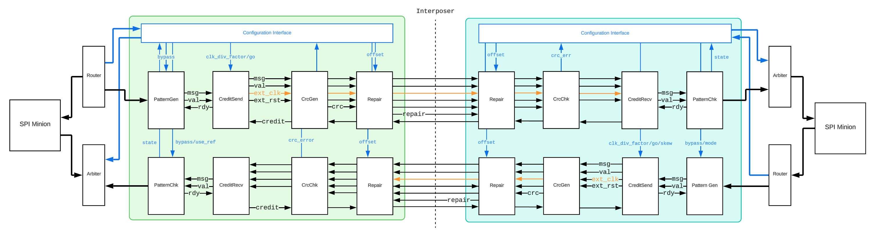
This is the home page for the BRGTC6 (Chip2Chip) project. In this project, we built a performant chip-to-chip communication interface. The taped-out test chip is a 1 mm², 200 MHz design in TSMC 65nm, and it achieved a throughput of 1.6 Gb/s at 200 MT/s in post-silicon testing.
Work in the project involved:
Designing a modular, performant, and open-source communication interface
Developing thoroughly tested RTL components
Setting up the TSMC 65nm PDK on the BRG server
Taping out a test chip in TSMC 65nm to demonstrate and validate our interface
GitHub page: BRGTC6 Repo
Full project report: BRGTC6: Source-Synchronous Parallel Chip-to-Chip Link
Timeline
2024
Jun 14 - Barry Lyu started working on the project
Jul 25 - Initial FPGA to FPGA demo
Aug 05 - First full architectural draft
Sep 18 - Parker Schless and Vayun Tiwari joined the project
2025
Jan 8 - V4 sent for tapeout
Spring - Chips received from fab
Chips successfully tested
Future Investigations / Revisions
Verification
Encapsulate testing system as a Verilog package so that it is portable
Allow for test case reuse across various modules
Handle build dependencies (do not recompile if nothing changed) for Verilator tests - see Aidan McNay’s Blimp project
RTL
Use modports and interfaces to encapsulate val/rdy and credit signals
PD
Add different standard views each configurable via a yaml file (e.g. for different corners, threshold voltages, etc.)
Support different MMMC corners during PnR
Background Information
RTL Design
Design Verification