BRGTC6 RTL Design Overview
SPI and Config Interface
The BRGTC6 chip can be configured from the outside by sending configuration requests through SPI. The SPI minion on the chip is a full duplex 20-bit interface with the top 2 bits used for a val/rdy protocol wrapper.
[19:18] |
[17] |
[16:12] |
[11:0] |
|---|---|---|---|
SPI Master Command / SPI Minion Status |
Destination Address
|
Config Interface Address
|
Config/Channel Value |
The address map of the configuration interface is HERE.
BRGTC6 Config Interface also provides documentation for all the configuration registers, their usage, and expected values.
Handling the Val/Rdy SPI Adapter
The val/rdy adapter for the SPI interface allows the minion to indicate its status to the master and thus allows it to negotiate with the master.
[19:18] |
[17:0] |
|---|---|
SPI Master Command / SPI Minion status |
Message |
For the master, the top 2-bits sent are used for the SPI Master Command:
SPI Master Command |
Usage |
|---|---|
2’b00 |
nocommand_read_msg |
2’b01 |
read_msg |
2’b10 |
write_msg |
2b’11 |
write_read_msg |
For the minion messages, the top 2-bits represent the internal status of the minion:
Bits |
Usage |
|---|---|
[19] |
Indicates whether the SPI minion has spaces left in the receiving buffer. if this is 0, then the message sent by write_msg in the next transaction might be dropped. |
[18] |
Indicates whether the SPI minion has a valid outgoing message for this transaction. |
A typical sequence for handling master and minion transactions with backpressure on the minion is:
SPI Master (Host computer):
Send a read_msg command with empty value.
Check the top two bits of the message from the minion
If the top-most ([19]) bit is 1, then the minion is ready
If the second to top ([18]) bit is 1, then this message from the minion is valid (it is a valid output and should be evaluated by the master)
Based on the minion response in the previous SPI exchange
If the minion is ready, send a write_msg command with the desired input. And jump to step 2.
Otherwise jump back to step 1.
See Integration Tests and check the GitHub repository for the associated files to see additional examples of configuration and chip usage through SPI messages
Link Config Example
Assuming the SPI val/rdy is handled correctly. A typical sequence for turning on the chip and enabling the PRBS auto-test for the link through the configuration interface:
Sending Chip:
Set the pattern mode to PRBS
Turn off the pattern bypass.
(Optionally) Configure clk skew and divisor
Set GO to 1.
Receiving Chip:
Turn off the pattern bypass
Poll for pattern state on the receiving chip
Link Specification
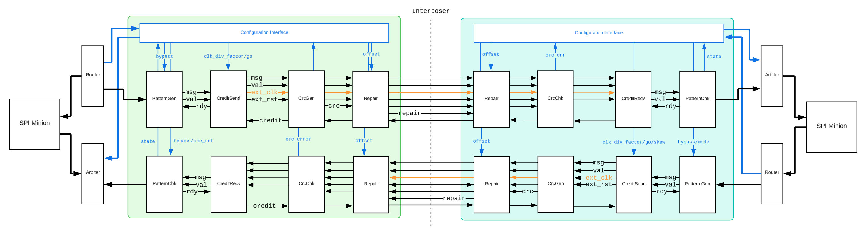
This diagram above shows the 2 V4 Links talking to each other. The core of the link is based on a source synchronous credit interface with five signals:
Signal |
Description |
|---|---|
cred_clk (upstream driven) |
The forwarded clk for sampling data |
cred_rst (upstream driven) |
The asynchronous link reset |
cred_msg (upstream driven) |
The message |
cred_val (upstream driven) |
Valid-bit for the message |
cred_cred (downstream driven) |
The returned credit |
A detailed description of transactions through the link:
Upstream Side:
Assert cred_rst
Start ticking cred_clk
Deassert cred_rst
Tick cred_clk for at least two more cycles (For the reset synchronizer on the downstream side to settle)
On a negedge of cred_clk: toggle the message and the valid bit
Reduce available credits by 1
Repeat 5-6 to send more messages, as long as available credits > 0
For every posedge of cred_cred, available credits increment by 2
Downstream Side:
cred_rst asynchronously resets the write and read ptr blocks of the async fifo.
upon two cycles of cred_clk after cred_rst is released, the async fifo comes out of reset
On posedge of cred_clk, take cred_msg in the fifo if cred_val is high.
Toggle cred_cred every time a message is taken out of the fifo.
Clock Domain Crossing
There is 1 CDC path in the upstream link, which converts cred_cred from an asynchronous clock signal to the core clk through a gray code synchronizer (a 0-bit async fifo).
There is also 1 CDC path in the downstream link, which converts messages from the cred_clk domain to the core clk domain through an async fifo.
Clock Divider and Skewer
CreditSend module has a builtin clock divider, which can divide cred_clk by any multiple of two if enabled, it can also “inject” artificial skew between cred_clk and cred_msg so that a skew in the physical connection path could be countered.
The clock divider is implemented with a counter that toggles the output clock every n cycle of the input clock.
The clock skewer is only functional when the clock divider is enabled. It doesn’t inject delays but rather changes at which cycle (in terms of core clock) the data is allowed to toggle, thereby creating different skew relationships between the data and the clock.
By default, the data is always toggled on the Negedge (when the clock divisor is set to 1, which just passes along the original clock)
Credit Interface
The credit interface used in the link is slightly modified for asynchronous credit return. In V3. we had a cred_cred toggle based on cred_clk, but this would break when the cred_clk is not divided and potentially faster than the core clock of the downstream.
Therefore we instead made an asynchronous credit return scheme where the credit is just toggled relative to the core clk of the downstream chip. The upstream is responsible for synchronizing and capturing the data.
This is done through the async counter module(an async fifo with just the pointer handling blocks and no memory), where the cred_cred signal is the input clock and the input valid is hardcoded to 1.
Because the downstream can only toggle the cred_cred signal from 1 to 0 or from 0 to 1 in any cycle, it only produces a posedge every two credits. To accommodate for this, every entry in the async counter module is worth 2 credits.
Reset Synchronizer
There are two types of reset synchronizes:
A 2DFF synchronizer for core logic reset. Synchronizes the reset signal coming from outside the chip.
An asynchronous reset synchronizer for synchronous release. Synchronizes the asynchronous reset from the other chip (It allows for asynchronous assertion but synchronizes the release).
Link Peripherals
PatternGen/Chk
The pattern generator and checker built into the link can be turned on to enable automated self-tests that stress test the link with PRBS or fixed pattern (alternates between two configured patterns).
The pattern mode and the fixed patterns can be set through the configuration interface. By default, pattern bypass is 1, which disables the pattern generator and checkers in the link.
CrcGen/Chk
A built-in CRC generator produces a single parity bit along with the message and checks it on the receiving side.
An error bit is set in the config interface if an error is detected, and is only reset to 0 upon a full-chip/credit-interface reset.
Repair
The repair unit adds an additional bit line to accommodate any broken pins, PCB connections, etc.
The offset can be set through the config interface to bypass any broken pin on the credit interface (clk, rst, val, cred, and each bit of msg).
In order for this to work, both sides of the link must have their repair offset set to the same value.